Today's circuits are like small boats swimming in a sea of electromagnetic (EM) energy that fluctuates widely in intensity and frequency. Electromagnetic interference (EMI), radio frequency interference (RFI), often grouped under the subject of electromagnetic compatibility (EMC), are ubiquitous and related phenomena that can affect the performance of circuits and official product compliance approval. While these issues have been a concern since the early days of electronics, the challenges they pose have become increasingly difficult due to the proliferation of wireless connectivity and the use of higher frequencies, more sensitive circuits, and lower voltage rails.
Interference affecting circuits may be caused by nearby intentional and
unintentional transmitters of electromagnetic energy, or may be caused by
natural or man-made sources. The circuit itself may also emit undesirable or
unacceptable electromagnetic energy, affecting nearby electronic equipment.
The most common solution to mitigate EMI/RFI energy issues is to add
shielding around critical components of the circuit board or even the entire
module. During the breadboard and prototype stages, this shielding can
provide temporary insight into the problem, mitigate it, and resolve it.
However, this ad hoc solution is not compatible with manufacturing
environments, or with testing, debugging and repair stations.
This article identifies fundamental EMC challenges for printed circuit
boards, components and products. Harwin's off-the-shelf shielding solutions
are then explored and how they can be used to improve technical
effectiveness and production compatibility.
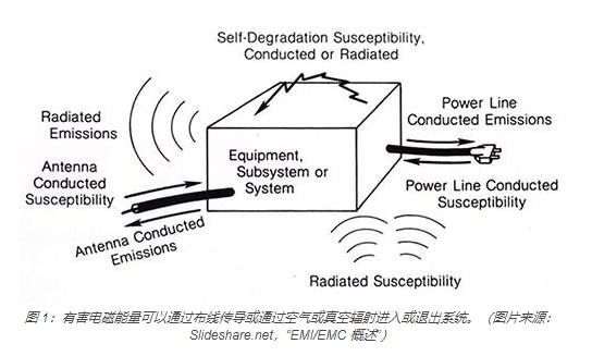
There are two ways EMC problems can arise
Electrical interference energy can be transferred from the source to the
"victim" circuit by conduction or radiation (Figure 1). In the case of
conduction, energy travels through conductors such as wires or cables.
Designers often use ferrite beads, filters, chokes, and other passive
components to attenuate this energy. In the case of radiation, the energy
path is through air or vacuum from source to victim, with no metallic
conductors.
These harmful effects can sometimes be reduced by relocating components at the source or victim, but this is a time-consuming process that is often impractical, impossible, or ineffective. Likewise, filtering is not a viable option because most of the interfering EMI/RFI energy is within the relevant operating radio frequency (RF) band, and filtering can reduce the strength of the desired signal and impact system performance.
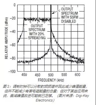
For some radiated EMI situations, a technique called "spread spectrum" is
sometimes used to reduce the peak EMI emissions at the operating frequency.
In this method, the circuit's clock randomly "jitters" around its nominal
frequency as a form of frequency hopping. This spreads the RF energy across
the spectrum, but it does not reduce the overall transmitted energy

Spread spectrum is considered a "cheat" by some
designers because it is done primarily to meet radiation limitations, while
others see it as a simple and effective solution. This approach is mainly
suitable for DC-DC switching regulators where fixed operating frequency is not
important; but for many situations where carrier and operating frequency
stability is critical, spread spectrum frequency hopping is not suitable.
Passive shielding: often the answer
In most EMC situations, interfering energy circuitry is beyond the control
of the designer, but it must be curtailed at the source or victim. An
effective and widely used solution for dealing with radiated EMI/RFI is to
add a grounded metal shield around the source of the interfering energy or
the victim, depending on the situation. This creates two engineering issues:
Which areas of the PCB need to be shielded?
How should this shielding be implemented in a production environment to
minimize time to market, cost, and impact on production?
In many cases, the area that needs shielding is obvious, such as the RF
transceiver section; in other cases, it takes many times the effort to find
the portion of the circuit that is emitting excessive EMI/RFI or is
susceptible to it. . To find these areas, designers typically build a small
EMI-enclosed conductive box that encloses and shields the area under
investigation. Depending on the product and design, the box may need to be
as small as a fingernail or large enough to surround the entire printed
circuit board.
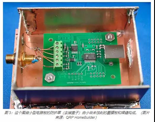
For smaller RF enclosures, thin copper sheets can be used to fold into
boxes, and the seams can be welded or covered with copper tape with
conductive glue. For medium and large enclosures, you can cut a scrap
copper-clad printed circuit board to the required size and then solder or
tape all the seams together with conductive tape. In some cases, the seams
are first "tack welded" to ensure basic stability, and then covered with
conductive tape.
The box is then placed over the area of the circuit board to be evaluated and
the seam line between the open bottom and the PCB is soldered to a low impedance
RF ground line. In practice, this can be more challenging than it seems because
the printed circuit board often does not yet have a corresponding ground trace
around the perimeter of the tank being built. While a few connection points may
be sufficient, a more continuous ground seam means there will be fewer RF
leakage paths into or out of the tank assembly.
There is another problem with this welding method. Since many PCBs have very
thin copper cladding, soldering or desoldering the test jar to the board will
most likely damage the delicate copper cladding and damage the board. Therefore,
before building and gluing these shielded cans, it's a good idea to take some
measurements of the situation using RF probes and sniffers.
A better way to prototype shielding
It is possible to create a shielded can using copper foil or copper-clad
printed circuit boards, but it is a time-consuming process. And there's the
FR-4 substrate to handle (if using PCBs), which is difficult to cut without
the right gear and leaves nasty fiberglass "shards" on your fingers unless
you wear gloves. Even using bare copper can be problematic, as you can cut
your fingers if not handled carefully, and a small bending machine may be
required to perform 90° bends on edges and corners. This DIY method for
making your own shielding test box may seem simple at first, but it's not as
quick and easy as it looks, although it certainly does work.
Consider RF attenuation and cooling factors
A fundamental practical problem with locating solid-surface metal cans
around circuit components is that they impede convective cooling airflow
over the surfaces of the enclosed components. It may seem that in many
applications the use of shielded cans should be ruled out, but this is not
the case. The reason is that the metal shell of the can is quite thin,
ranging from 0.15 to 0.3 mm depending on the specific model and
specification of the can. This thickness creates only a small obstacle to
the conduction of heat from the inside of the jar to the outside. Once the
heat reaches the outer surface of the can, it can be dissipated through
natural or forced air convection or other means.
In this regard, the thermal performance of a thin metal can is much better
than a shielded enclosure made of ordinary FR-4 PCB material. The latter has
a thermal conductivity between 1 and 3 Watts/meter-Kelvin (W/m-K) and a
standard thickness of 1.6 mm, so the thermal resistance is much higher.
Compare this number to the thermal conductivity of nickel silver, which is
about 1000 times more conductive and much thinner (only 0.15 to 0.3 mm). The
effect of thin metal cans on cooling can be quantified through basic thermal
modeling. Alternatively, standard techniques can be used to take advantage
of the high thermal conductivity of the underlying printed circuit board
copper to remove large amounts of heat from the mounted components. This is
a good practice in almost all situations.
An obvious solution to improve heat convection in a shielded tank is to make
holes in the surface of the tank. However, this adds another Product
New question. The holes must be small enough and spaced far enough apart,
otherwise there may be radio frequency leakage. Since the maximum allowable
diameter and spacing are a function of wavelength, the most straightforward
requirement is that any opening must not exceed one-tenth of the shortest
wavelength of the RF being shielded.
However, determining critical wavelength and hole size is not always easy or
obvious because the frequency of interfering RF energy may be higher (and
therefore shorter wavelength) than the product's apparent operating
frequency or carrier frequency. Given that interfering gigahertz frequency
signals can overload and saturate nearby megahertz frequency front-end
amplifiers, the maximum allowable aperture must be much smaller than a
simple preliminary analysis of the product's operating frequency would
determine.
Keep in mind that in addition to ensuring circuit performance, another goal
of shielding cans and clamps may be to provide RF attenuation over a wide
frequency range to meet regulatory requirements for the product. These
EMC-related regulatory standards define the maximum RFI/EMI that a product
can generate in various regions of the radio frequency spectrum, as well as
the permissible susceptibility of a product to being an EMI/RFI victim,
regardless of the nominal operating frequency.
Therefore, shielding must typically not only guarantee performance at the
apparent operating frequency, but must also provide attenuation across the
broader EM spectrum. Using cooling holes sized only for the nominal
operating frequency may reduce the attenuation of those shorter wavelength
spectrum and may affect regulatory approval.
Conclusion
Electromagnetic compatibility and RFI/EMI issues affect nearly all
electronic products and applications, and the increasing use of higher
frequency wireless links makes design even more challenging. Radiated
EMI/RFI causes many problems, and the solution often involves basic RF
shielding, which involves using a metal can to completely enclose the
affected circuit.
The cans are available as standard in a variety of sizes, with PCB clamps
available in a variety of configurations to allow the cans to be easily
snapped onto or removed from the circuit board. The clamps are also fully
compatible with equipment used for inserting and soldering SMT packaged
components in volume production environments.